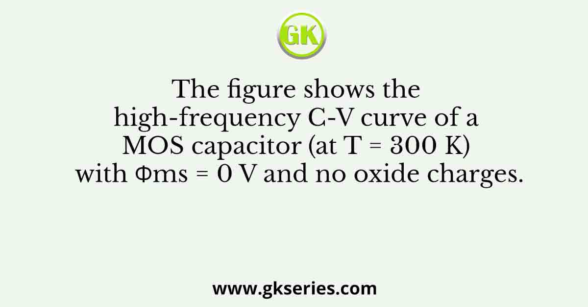
Q. The figure shows the high-frequency C-V curve of a MOS capacitor (at T = 300 K) with Φms = 0 V and no oxide charges. The flat-band, inversion, and accumulation conditions are represented, respectively, by the points

(A) P, Q, R
(B) Q, R, P
(C) R, P, Q
(D) Q, P, R
Ans: Q, R, P
Solution:
1) Flat band voltage is the voltage where there is a no-charge present in the oxide or oxide semiconductor interface. 2) As the gate voltage Va increase, more electrons are attracted to the oxide-semiconductor interface. A-n type channel is formed. The inversion takes place at R 3) For negative gate voltage, more holes are accumulated near the gate. Accumulations take place at P.


![Determine the correctness (or otherwise) of the following Assertion [A] and the Reason [R]](https://www.gkseries.com/blog/wp-content/uploads/2023/10/Determine-the-correctness-or-otherwise-of-the-following-Assertion-A-and-the-Reason-R.jpg)